


Cellular microstructures form naturally in many living organisms (e.g., flowers and leaves) to provide diverse and vital functions in their 3D shape formation, synthesis/transport of nutrients, and regulation of growth/reproduction. Owing to the light weight and high strength, high specific surface area, and excellent thermal properties of cellular structures, bio-inspired cellular designs have been exploited in the development of materials and functional systems. Examples include lattice materials and foams with high specific stiffness/strength, artificial tissues/organs with hierarchical vascularized networks and electromagnetic metamaterials. However, the shape programming for 3D curved mesosurfaces through biomimetic cellular microstructures remains unexplored. The design and fabrication of 3D curvy electronic devices with programmable curvatures to meet the specific application demands, play important roles in bioelectronics, micro-robotics, nanooptics, among others.
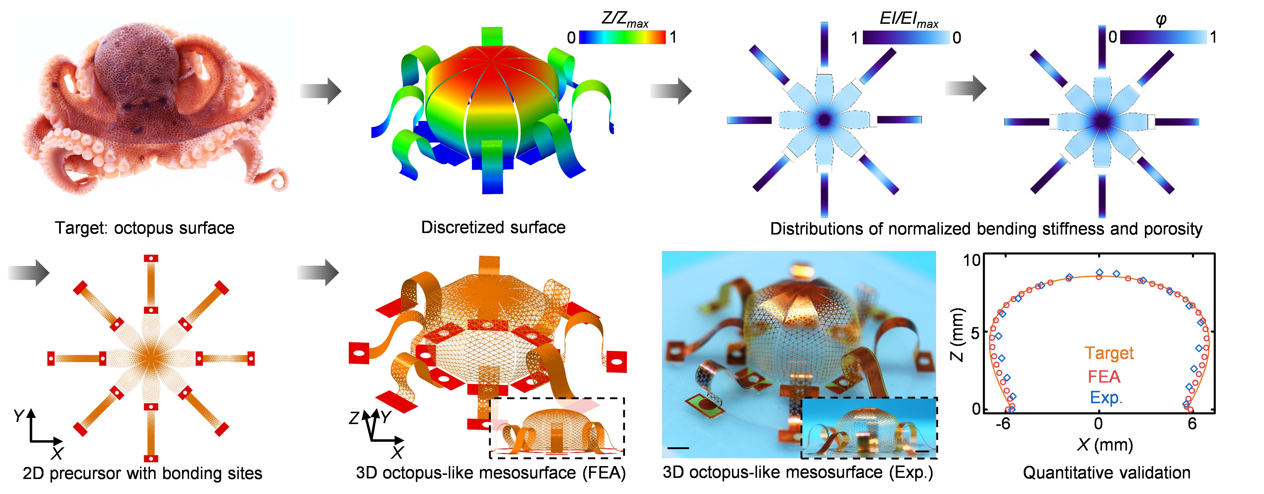
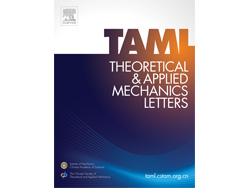
Figure 1. Design and assembly of an octopus-likemesosurface based on the microlattice strategy.
Recently, inspired by cellular biological surfaces, TAML editorial board member Prof. Yihui Zhang at Tsinghua University and his collaborators developed a microlattice design as a powerful route to achieve desired stiffness distribution of 2D micro-films, thereby allowing their transformation into programmable 3D curved mesosurfaces through the mechanically-guided assembly (Fig. 1). Both an analytical model and a machine-learning-based computational approach are established for the inverse design of target 3D curved mesosurfaces from 2D microlattice patterns with optimized distributions of porosity and cell sizes. Compared with the reported design strategies through thickness engineering, the microlattice design bypasses the technical challenges in finely tuning the thickness distribution of micro-films.
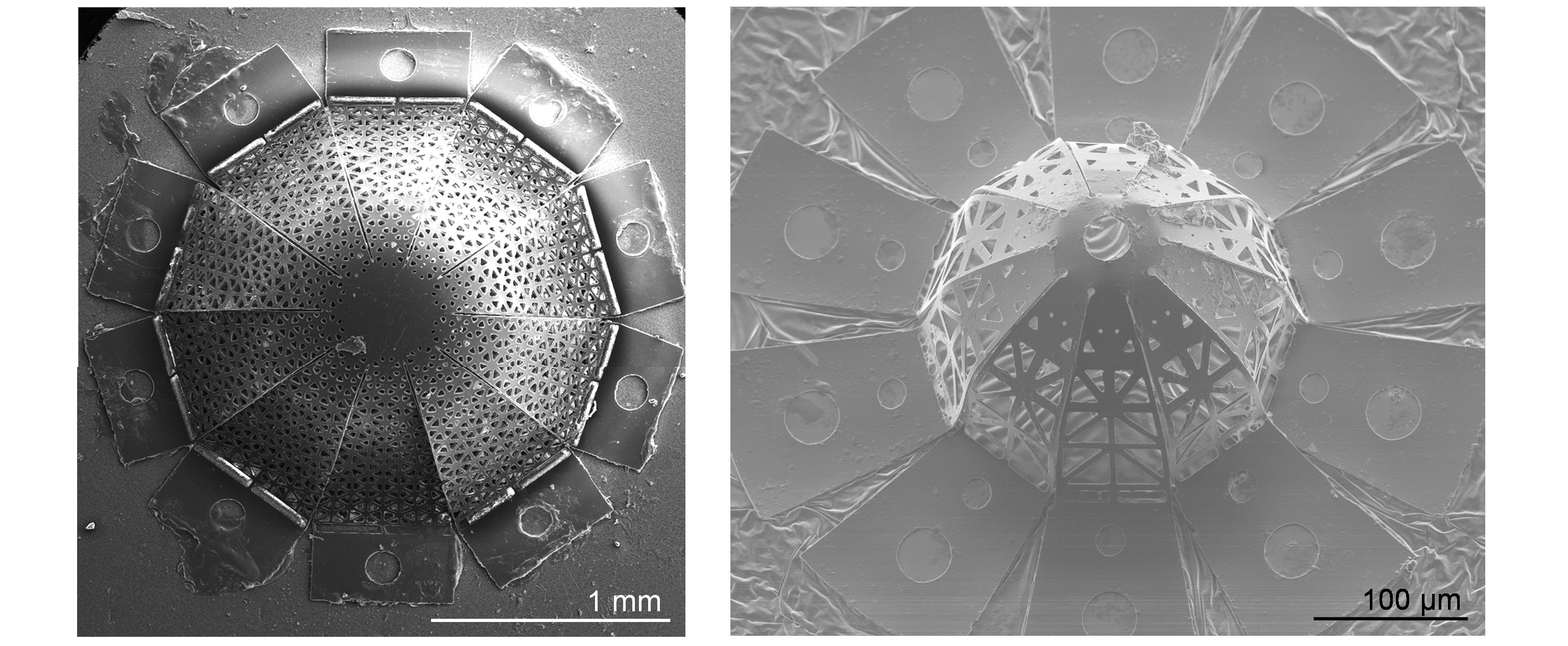
Figure 2. Assembly of a spherical cap and a hemisphericalmesosurface based on the microlattice strategy.
With the developed microlattice designs, this work presents the rational assembly of over 30 examples, including regular curved mesosurfaces (e.g., hemispherical, hemi-ellipsoidal, and hemi-toroidal surfaces) and complex biological mesosurfaces (e.g., flower-/fruit-like plant surfaces, and ant-/octopus-/stingray-like animal surfaces), in diverse materials (e.g., silicon, metal, chitosan, polyimide and laser-induced graphene), with feature sizes spanning from ~ 2.7 μm to 30 μm in film thickness, and ~ 250 μm to 30 mm in lateral dimension (Figs. 2 and 3).
Figure 3. Assembly of two flower-like mesosurfaces withbonding sites distributed inside the microlattice.
The bioinspired microlattice designs allow construction of 3D electronic systems with desired curvature distributions. Demonstrations of conformable cardiac electronic device, stingray-like dual-mode actuator and 3D electronic cell scaffold (Fig. 4) suggest rich opportunities in practical applications.
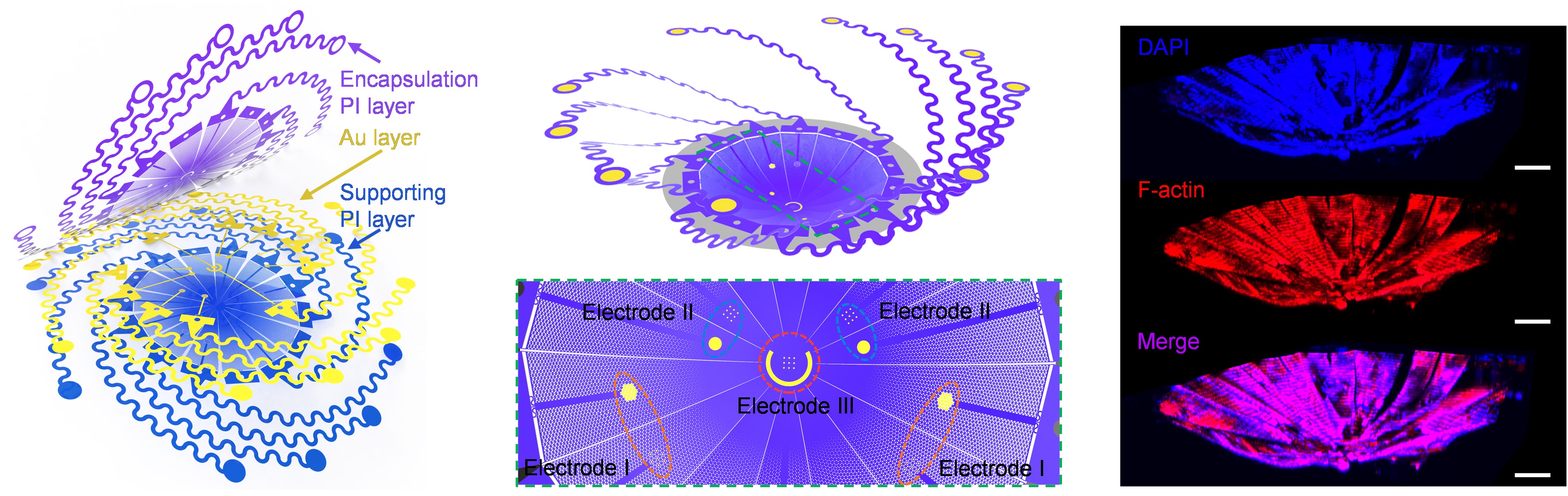
Figure 4. A 3D electronic cell scaffold mimickingthe retina based on the microlattice strategy.
This work was published last week in Science as a Research Article entitled “Programming 3D Curved Mesosurfaces using Microlattice Designs”. Prof. Yihui Zhang is the corresponding author, and Dr. Xu Cheng and Prof. Zhichao Fan are co-first authors of the paper. A few days after the publication, Nature published a Research Highlight “Life’s wondrous forms recreated in graphene and more” about this work.
More information: Xu Cheng et al, Programming 3D curved mesosurfaces using microlattice designs, Science 379, 1225 (2023). DOI: 10.1126/science.adf3824
 Submit a Paper